Rochester Electronics NB7N017MMN especificações técnicas, atributos, parâmetros.
Category:Integrated Circuits (ICs)/Clock Generators, PLLs, Frequency Synthesizers
製品ステータス:Obsolete
動作温度:-40°C ~ 85°C
取り付けタイプ:Surface Mount
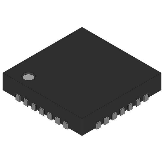
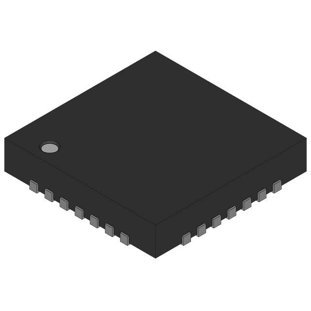
パッケージ/ケース:52-VFQFN Exposed Pad
タイプ:Clock Divider
サプライヤーデバイスパッケージ:52-QFN (8x8)
周波数 - 最大:3.5GHz
回路数:1
出力:CML
電圧 - 供給:3V ~ 3.465V
PLL:No
入力:CML, ECL, LVCMOS, LVDS, LVTTL
比率 - 入力:出力:1:1
差動 - 入力:出力:Yes/Yes
除算器/乗算器:Yes/No
EU RoHS ステータス:RoHS non-compliant
モイスチャーレベル:2 (1 Year,30°C/60%RH)
REACH規則:REACH Unaffected
輸出規制分類番号:EAR99
HTS 米国:8542.39.0001
中国の RoHS ステータス:Orange Symbol: Safe for use during the environmental protection period
Rochester Electronics NB7N017MMN Detalhes
Overview of Onsemi NB7N017MMN
The Onsemi NB7N017MMN is a high-performance low-skew differential driver and fanout buffer that is suitable for clock and data distribution applications in high-speed digital circuits. It is designed to provide precise timing and low skew between output signals. The device is typically used in communication systems, data centers, imaging applications, and other digital systems requiring clock distribution at high frequencies.
Functions of Onsemi NB7N017MMN
1. Low-Skew Clock Distribution: The primary function of the NB7N017MMN is to buffer and distribute clock signals with minimal skew, ensuring that signals reach their destinations with precise timing.
2. High-Speed Performance: The IC operates at high frequencies, making it suitable for applications that demand fast data processing speeds.
3. Differential Signaling: It uses differential signaling to improve noise immunity and signal integrity, especially in long transmission lines.
4. Fanout Capability: The device can drive multiple outputs from a single input, allowing for flexible circuit designs where one clock source needs to be distributed to many destinations.
5. Single-ended to Differential Conversion: Provides functionality to convert a single-ended input signal to a differential output.
Applications of Onsemi NB7N017MMN
1. High-Speed Data Communications: Utilized in routers, switches, and other networking equipment to ensure synchronized clock signal distribution.
2. Cloud Computing: Used in data centers to facilitate high-speed interconnects and communication between devices.
3. Telecommunications: Adopts in telecom equipment to maintain signal integrity over long distances.
4. Imaging Applications: Ideal for applications where precise timing is critical, such as in camera systems and image processing units.
5. Consumer Electronics: Employed in high-performance gaming systems, set-top boxes, and other consumer devices requiring high-speed data processing.
Alternative Components
1. Texas Instruments TXS0108E: An 8-channel bidirectional level shifter that supports high-speed applications.
2. NXP 74LVC1G34: A single Schmitt trigger buffer designed for high-speed signal buffering.
3. Maxim Integrated MAX3402E: A multidrop RS-485 transceiver equipped with low skew capabilities for communication applications.
4. ON Semiconductor NB7V12M: A similar device with fanout buffer capabilities, focused on clock distribution.
5. Analog Devices ADCLK846: An ultra-low skew clock buffer optimized for high-performance communication applications.
Embedded Modules
The Onsemi NB7N017MMN can be incorporated into various embedded systems within modules such as:
1. FPGA Development Boards: Often used in conjunction with field-programmable gate arrays to manage clock distribution.
2. High-Performance Microcontroller Boards: Utilized in embedded applications requiring clock distribution for precision timing.
3. Communication Interface Modules: Used in interfaces such as USB3.0 or PCIe, where precise timing is crucial.
4. Signal Conditioning Modules: For enhancing and managing signals in data acquisition systems.
5. IoT Gateway Devices: Ensuring that high-speed communications are maintained in Internet of Things applications.
Related Q&A
1. Q: What is the maximum input frequency for the NB7N017MMN?
- A: The maximum input frequency is typically around several GHz, depending on the specific application, but data sheets should be referenced for exact specifications.
2. Q: Can the NB7N017MMN function in single-ended applications?
- A: While the NB7N017MMN is primarily designed for differential signaling, it can be used in single-ended applications with proper termination.
3. Q: What is 'low skew' and why is it important?
- A: Low skew refers to the minimal time difference between clock signals at various outputs. It is crucial for synchronous operation in digital systems to avoid data corruption.
4. Q: How do I power the NB7N017MMN?
- A: The NB7N017MMN requires a specific voltage supply as detailed in its datasheet, typically around 3.3V or 2.5V, with proper decoupling capacitors.
5. Q: What considerations must be made for PCB layout with the NB7N017MMN?
- A: It is critical to minimize trace lengths, maintain signal integrity with controlled impedance, and properly route differential pairs to reduce skew and improve performance.
This overview and related information should provide you with a solid understanding of the Onsemi NB7N017MMN and its context in integrated circuits.


 NB7N017MMN Ficha de dados